
The human brain is a product of evolution, tuned and reshaped by an ever-changing environment. The brain’s neuronal system is able to achieve the ability to recognize, conceptualize and memorize objects in the physical world. Using environmental information we establish logical associations that ultimately allows us not only to survive, but also to solve highly complex problems1.However, in an increasingly connected and interactive world, the volume of information to process has exponentially increased, and in order to extract and synthesize meaningful information, computerized approaches, such as machine learning and its various incarnations have gained tremendous popularity2.
Typically, Artificial Neural Networks (ANNs) attain this goal by a very delicate and case-selective combination of learning strategies3. Data containing complex or contextual associations between objects normally requires an heuristic sampling which limits their ability to synthesize information. Conventional CMOS architectures also restrains the amount of data that is efficiently processed with ANNs due to power consumption bottlenecks.
Interest in the creation of synthetic neurons that could increase the processing abilities of ANNs has increased considerably with the discovery of nanomaterials with memristive properties4. A memristive device is a non-linear two-terminal device in which the resistance shows resilience to change (i.e. memory), manifested in hysteretic behavior when the energy change is reversed or reduced, also termed as resistive switching. The memristor thus has two important neurosynapse-like properties, plasticity and retention. Traditional integrate-and-fire models, that emulate the electrical behavior of neurons using passive circuit elements, can be simulated exclusively with these elements5,6,7. Memristive devices have been successfully embedded into various CMOS architectures, enabling the realization of synthetic neural networks(SNN). SNNs imitate the topology of an ANN in a physical layout, typically stacking memristive terminals in cross-bar configurations8,9. Using voltage pulses to configure the internal state, or weight, of individual memristors; memorization, learning and classification abilities have been achieved10,11,12,13. However promising, this approach remains reliant upon CMOS technology and inherits some of its limitations: large cost-efficiency ratio, high power consumption, and subpar performance with respect to computerized ANNs …..
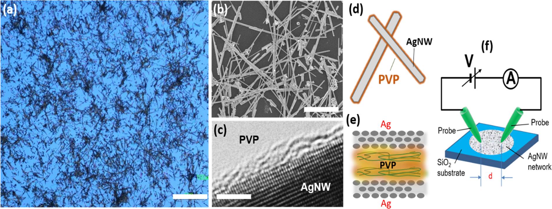
Morphological and structural properties of PVP-coated Ag nanowires and nanowire network. (a) Optical micrograph image of nanowire network layout after drop-cast deposition on a SiO2 substrate. (b) SEM image of nanowire interconnectivity in a selected area of the network. (c) HR-TEM image showing the atomic planes of the [100] facet of a Ag nanowire with the nanometric PVP layer embedded on the lateral surface of the nanowire. Figures (d,e) sketch the detail of the insulating junctions formed by the polymeric PVP layer between the Ag surfaces of overlapping nanowires. (f) Scheme of the measurement system. Two tungsten probes, separated by distance d = 500 μm, act as electrodes, contacting the nanowire network deposited on SiO2. The scale bars for figures (a–c) are 100 μm, 10 μm and 2 nm, respectively.
Read full post: https://www.nature.com/articles/s41598-019-51330-6